Document Number: 69062
S10-1367-Rev. D, 14-Jun-10
www.vishay.com
3
Vishay Siliconix
SiC417
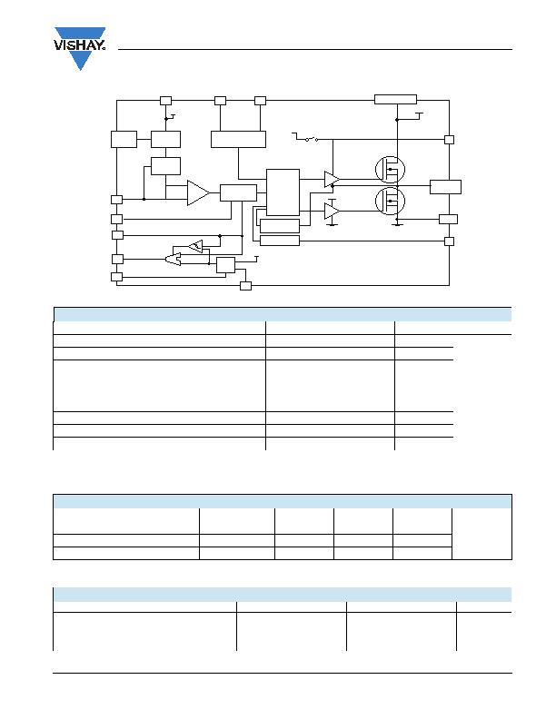
FUNCTIONAL BLOCK DIAGRAM
Stresses beyond those listed under "Absolute Maximum Ratings" may cause permanent damage to the device. These are stress ratings only,
and functional operation of the device at these or any other conditions beyond those indicated in the operational sections of the specifications is
not implied. Exposure to absolute maximum rating/conditions for extended periods may affect device reliability.
Note:
For proper operation, the device should be used within the recommended conditions.
V
IN
V
IN
6, 9 - 11 PAD 3
BST
LX
13, 23 - 25
28, PAD 3
P
GND
15-22
I
LIM
27
V5V
DL
V5V
ENL
32
V
IN
LDO
MUX
Y
A
B
FBL
V
LDO
V
OUT
t
ON
FB
2
7
5
1
31
Soft Start
A
GND
3
26
29
Control and Status
Valley 1 - Limit
Zero Cross
Detector
Gate Drive
Control
Reference
1.20.21
PAD 1
+
-
FB Comparator
Bypass Comparator
V5V
V5V
PGD
EN/PSV
8
ABSOLUTE MAXIMUM RATINGS T
A
= 25 癈, unless otherwise noted
Parameter
Symbol
Min.
Max.
Unit
LX to P
GND
Voltage
V
LX
- 0.3
+ 30
V
LX to P
GND
Voltage (transient - 100 ns)
V
LX
- 2
+ 30
V
IN
to P
GND
Voltage
V
IN
- 0.3
+ 30
V
EN
Maximum Voltage
V
EN
- 0.3
V
IN
BST Bootstrap to LX; V5V to P
GND
- 0.3
+ 6.0
A
GND
to P
GND
V
AG-PG
- 0.3
+ 0.3
EN/PSV, P
GOOD
, I
LIM
, V
OUT
, V
LDO
, FB, FBL to GND
- 0.3
+ (V5V + 0.3)
t
ON
to P
GND
- 0.3
+ (V5V - 1.5)
BST to P
GND
- 0.3
+ 35
RECOMMENDED OPERATING CONDITIONS
Parameter
Symbol
Min.
Typ.
Max.
Unit
Input Voltage
V
IN
3.0
28
V
V5V to P
GND
V5V
4.5
5.5
V
OUT
to P
GND
V
OUT
0.5
5.5
THERMAL RESISTANCE RATINGS
Parameter
Symbol
Min.
Typ.
Max.
Unit
Storage Temperature
T
STG
- 40
+ 150
癈
Maximum Junction Temperature
T
J
-
150
Operation Junction Temperature
T
J
- 25
+ 125
发布紧急采购,3分钟左右您将得到回复。
相关PDF资料
SP619EK-L/TR
IC HIGH CURRENT SW SOT23-6
TC573302ECTTR
IC REG CTRLR SGL 3.3V SOT23A-5
TC670ECHTR
IC FAN FAILURE DETECTOR SOT23A-6
TC74A7-5.0VCTTRG
IC DGTL THERM SNSR 5.0V SOT23A-5
TC77-5.0MOATR
IC THERMAL SENSOR SPI 5V 8-SOIC
TC9402EJD
IC V-FREQ/FREQ-V CONV 14CDIP
TCN75-5.0MUAG
IC TEMP SENSOR SRL 5.0V 8MSOP
TEA1750T/N1,518
IC PFC CONTROLLER DCM16SOIC
相关代理商/技术参数
SIC417DB
制造商:Vishay Intertechnologies 功能描述:
SIC424
制造商:VISHAY 制造商全称:Vishay Siliconix 功能描述:6 A, microBUCK SiC414, SiC424 Integrated Buck Regulator with 5 V LDO
SIC424CD-T1-GE3
功能描述:直流/直流开关调节器 6A 16 V with Program LDO
RoHS:否 制造商:International Rectifier 最大输入电压:21 V 开关频率:1.5 MHz 输出电压:0.5 V to 0.86 V 输出电流:4 A 输出端数量: 最大工作温度: 安装风格:SMD/SMT 封装 / 箱体:PQFN 4 x 5
SIC711CD10-T1
制造商:Vishay Siliconix 功能描述:FAST SWITCHING MOSFETS W/INTEG DRIVER - Tape and Reel 制造商:Vishay Siliconix 功能描述:MOSFET N POWERPAK
SIC714CD10
制造商:VISHAY 制造商全称:Vishay Siliconix 功能描述:Fast Switching MOSFETs With Integrated Driver
SIC714CD10-T1
制造商:Vishay Siliconix 功能描述:FAST SWITCHING MOSFETS W/INTEG DRIVER - Tape and Reel 制造商:Vishay Siliconix 功能描述:IC MOSFET DRIVER N-CH 68MLF 制造商:Vishay Siliconix 功能描述:MOSFET N POWERPAK
SIC714CD10-T1-E3
制造商:VISHAY 制造商全称:Vishay Siliconix 功能描述:Fast Switching MOSFETs With Integrated Driver
SIC73
制造商:未知厂家 制造商全称:未知厂家 功能描述:Low Profile (2.5mm max, height) SMD type